


Inside Intels Chip Creation and Innovation
by Jeffrey Burt
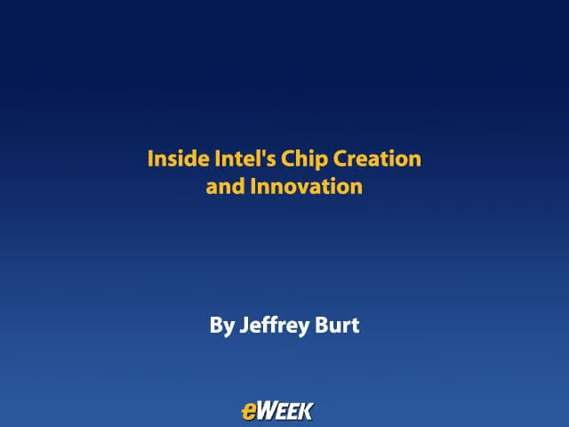
Starting with Sand
Sand is the base ingredient for semiconductor manufacturing, given its high percentages of silicon. The silicon is purified through multiple steps to reach a semiconductor manufacturing quality called Electronic Grade Silicon, which means there can only be one alien atom every 1 billion silicon atoms. In the second image, one big crystal is grown from the purified silicon melt. In the last image is an ingot that has been produced from Electronic Grade Silicon. One ingot weighs about 220 pounds.
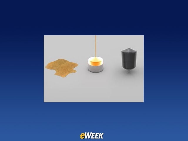
Slicing the Ingot
The ingot is cut into wafers, which are single silicon disks. As seen in the second image, the wafers are then polished until they have flawless and mirror-smooth surfaces. Intel buys the manufacturing-ready wafers from third-party suppliers. In its 45-nanometer manufacturing process, Intel uses wafers with diameters of 300 millimeters, or about 12 inches.
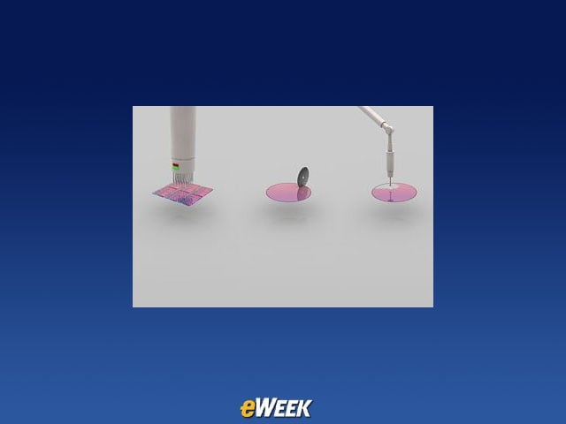
Getting to the Transistor
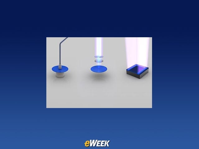
The blue liquid in the first image is a photo-resist finish that is poured onto the wafer while it spins. In the second image, the the photo-resist finish–which is similar to the finish used in film photography–is exposed to ultraviolet light, which makes the finish soluble. Then masks–which act like stencils–are used with the UV light to create circuit patterns on each layer of the microprocessor. A lens, seen in the middle of the UV light, reduces the mask’s image to the point that what gets printed on the wafter is about four times smaller than the pattern on the mask. The third image shows a transistor, which controls the flow of electrical current in the chip. Intel has developed transistors so small that about 30 million of them can fit on the head of a pin.
Removing the Photo Resist
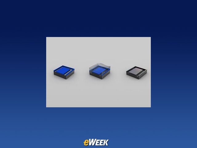
In the first image, a solvent is used to dissolve the gooey photo resist, revealing the pattern of photo resist made by the mask. Chemicals are then used to etch away material revealed by the dissolved photo resist, and, finally, the photo resist is removed and the desired shape of the transistor becomes visible, as seen in the third image.
Implanting the Ions
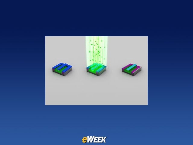
Photo resist, in blue, is applied. The photo resist protects material that should not get ions implanted on it. In the second image, through a process called ion implantation–one form of a process called “doping”–the exposed areas of the wafer are bombarded with ions, which are various chemical impurities that alter the way silicon in these areas conduct electricity. The ions are shot into the wafer’s surface at speeds of about 185,000 mph. After the doping process, the photo resist is removed.
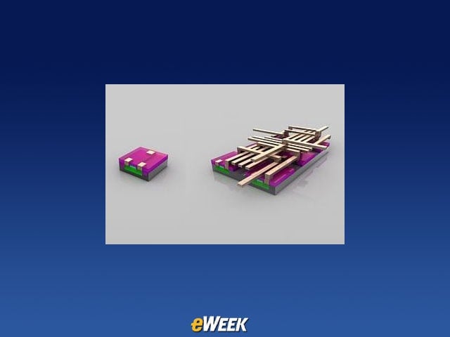
Putting on the Copper
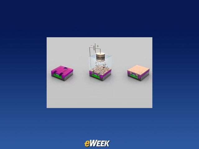
The transistor in the first image is close to being finished, and three holes have been etched into the insulation layer–in magenta–above it. The holes will be filled with copper for connections to other transistors. In the second image, transistors–which at this point are still on the wafers–are put into a copper sulphate solution, where copper ions are put onto the transistor through the electroplating process. After the electroplating, the copper ions settle on the wafer surface as a thin layer of copper.
Applying the Metal
The excess material is polished off, as seen in the first image. Then metal layers are created for interconnects between the various transistors. The chip’s architecture and design teams will determine how the connections are made. Though they appear flat, chips can have more than 20 layers in order to create their circuitry.
Finding the Right Answer
Wafers now undergo their first functionality tests, where test patterns are fed into every chip. The response from the chip is then monitored and compared to what engineers say is the “right answer.” As seen in the second image, the wafer is then cut into pieces, called dies. Then the dies with the right answer to the test pattern are sent forward to the next step, which is packaging. Faulty dies–those that did not respond with the right answer–are discarded.
Completing the Process
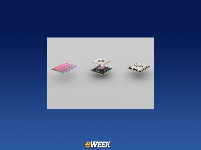
The first image shows an individual die–in this case, a die of an Intel Core i7 chip–cut from the wafter. Then the substrate, the die and the heatspreader are put together to create a completed processor. The substrate, in green in the second image, creates the electrical and mechanical interface through which the chip interacts with the rest of the PC system, and the silver heatspreader will be covered with a cooling solution to keep the processor cool while it’s operating. The end result is the completed processor, shown in the third image.
Preparing for Retail
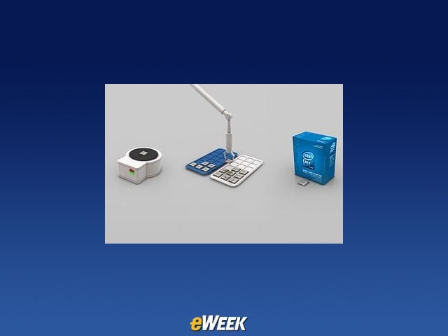
The chip goes through its final tests for such key characteristics as power dissipation and maximum frequency. As shown in the second image, processors with the same capabilities–as determined through class testing–are put into the same transporting trays. Finally, the manufactured and tested chips are sent to system manufacturers in trays or to retail stores in a box, as shown in the third image.